My Research Interest
Synthesis of Single-Walled Carbon Nanotubes
Since their discovery, Single Wall Carbon Nanotubes (SWCNTs) have attracted the interest of Materials Scientists, Physicists, Chemists and other researches due to their extraordinary properties. It has been suggested that they may be used in promising breakthrough applications such as space elevators, artificial muscles, ultrahigh-speed flywheels, and more. Researchers at MIT are working on combat jackets utilizing carbon nanotubes for ultrastrong fibers and for monitoring the wearer's condition. There are multiple ways of SWCNT preparation, the most common are Arc-Discharge (AD), Chemical Vapor Deposition (CVD) and Laser Ablation (LA).
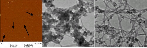
In Arc-Discharge we pass high current (approx. 100 A) across two metal doped graphite electrodes placed in a water cooled steel reactor filled with inert gas at low pressure (200-800 mBar). The relative simplicity of the AD method is balanced by the rather limited purity of the material produced (see Fig. 1).
Still, such material is the most common, and it is the only one available in relatively large batches (100g). Moreover, its purity is sufficient for many applications, such as conductive composite reinforcement, thin films or electrostatic shielding. We set-up the AD reactors at Stuttgart and Shanghai and we are routinely producing large batches of SWCNTs for research purposes.
The Chemical Vapor Deposition (CVD) method is based on catalytic decomposition of gaseous carbon feedstock mixed with inert gas and hydrogen. CVD is a promising method for large scale SWCNT preparation but we focused on growth of nanotubes on substrates, namely on Si/SiO2, widely used in electronics. We can grow extremely long isolated SWCNTs, excellent for transport measurement, as shown in Fig. 1. Here ethanol was used as the carbon source and a mixture of H2 and Ar as the carrier gas. The clear advantage of CVD is growth of nanotubes with little or no amorphous coating and the fact that they are already placed on a silicon chip surface. Thus they do not need further manipulation, which may lead to contamination, damage or change of properties. CVD is the most likely method to be used for combining carbon with conventional silicon based technology for near-future microelectronics.
For applications where high purity is mandatory and for reference purposes, Laser Ablation (LA) is the method of choice. In conventional LA apparatus we hit a heated, metal doped graphite target with focused laser pulses, which leads to vaporization of carbon (see Fig. 2).
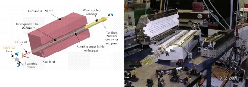
We improved the Laser Ablation set-up by adding an additional CO2 laser, used for after-heating of the plasma plume and thus slowing-down the cooling rate, which prolongs the growth phase. Such improvement results in a higher ablation rate and purity of the prepared SWCNT material. The improved purity was confirmed by Transmission Electron Microscopy (see Fig.1), termogravimetry and by VIS/NIR spectroscopy.
We set-up all three methods of SWCNT preparation, and succeeded in producing nanotube samples. In the case of Arc-Discharge, we optimized the process conditions so that we are able to deliver 100+ g batches for application studies. In the case of Laser Ablation, we improved the initial set-up so that now we have a much higher purity and ablation rate. In the case of CVD, we succeeded in the growth of long and isolated SWCNTs that are excellent for the study of transport properties.
Diffractive microoptical elements & holographic recording
My former research was focused on amorphous (unordered or glassy) thin films. We used amorphous chalcogenides which are oxide-like compounds as, for example As2S3 or As2Se3. They are photosensitive, so one can employ them as holographic medium. Their chemical resistance depends on exposure so, we may fabricate not only amplitude but also phase gratings.
We used holographic exposures and visible laser lithography to make elements such as gratings, artificial holograms and Fresnel lenses.

One can easily achieve feature size below the wavelengths of use radiation, theoretically down to half of wavelength. Results of my research are concluded in my Master (Dipl. Ing.) Thesis:
Forming of diffractive elements in thin amorphous chalcogenide layers